- 您现在的位置:买卖IC网 > Sheet目录314 > AT93C46Y6-10YH-1.8 (Atmel)IC EEPROM 1KBIT 2MHZ 8DFN
AT93C46
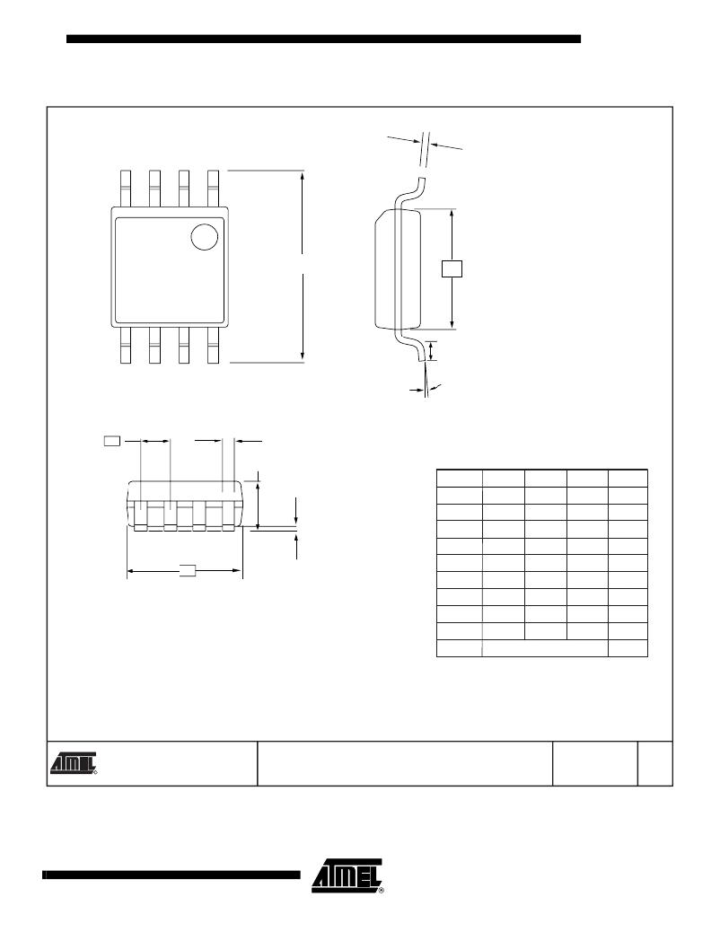
8S2 – EIAJ SOIC
C
1
Top View
N
E
E1
L
?
End View
e
A
b
COMMON DIMENSIONS
(Unit of Measure = mm)
A1
SYMBOL
A
A1
b
C
MIN
1.70
0.05
0.35
0.15
NOM
MAX
2.16
0.25
0.48
0.35
NOTE
5
5
D
Side View
D
E1
E
L
5.13
5.18
7.70
0.51
5.35
5.40
8.26
0.85
2, 3
?
e
0?
1.27 BSC
8?
4
Notes: 1.
2.
3.
4.
5.
This drawing is for general information only; refer to EIAJ Drawing EDR-7320 for additional information.
Mismatch of the upper and lower dies and resin burrs are not included.
It is recommended that upper and lower cavities be equal. If they are different, the larger dimension shall be regarded.
Determines the true geometric position.
Values b and C apply to pb/Sn solder plated terminal. The standard thickness of the solder layer shall be 0.010 +0.010/ ? 0.005 mm.
10/7/03
R
2325 Orchard Parkway
San Jose, CA 95131
TITLE
8S2 , 8-lead, 0.209" Body, Plastic Small
Outline Package (EIAJ)
DRAWING NO.
8S2
REV.
C
13
5140B–SEEPR–2/07
发布紧急采购,3分钟左右您将得到回复。
相关PDF资料
AT93C56A-10TU-2.7
IC EEPROM 2KBIT 2MHZ 8TSSOP
AT93C86AY6-10YH-1.8
IC EEPROM 16KBIT 2MHZ 8MAP
ATAVRBFLY
KIT EVALUATION AVR BUTTERFLY
ATAVRXBNDL
XMEGA XPLAIN AND DISPLAY MODULE
ATDH2222
ADAPTER FOR ATDH2200 20PLCC
ATDH2225
CABLE ISP FOR AT17
ATDH2227
ADAPTER FOR ATDH2200 44PLCC
ATEVK1101
KIT DEV/EVAL FOR AVR32 AT32UC3B
相关代理商/技术参数
AT93C56
制造商:ATMEL 制造商全称:ATMEL Corporation 功能描述:Three-wire Serial EEPROMs
AT93C56-10PA-2.7C
制造商:未知厂家 制造商全称:未知厂家 功能描述:Microwire Serial EEPROM
AT93C56-10PA-5.0C
制造商:未知厂家 制造商全称:未知厂家 功能描述:Microwire Serial EEPROM
AT93C56-10PC
功能描述:电可擦除可编程只读存储器 1/2/4k 3-Wire Bus
RoHS:否 制造商:Atmel 存储容量:2 Kbit 组织:256 B x 8 数据保留:100 yr 最大时钟频率:1000 KHz 最大工作电流:6 uA 工作电源电压:1.7 V to 5.5 V 最大工作温度:+ 85 C 安装风格:SMD/SMT 封装 / 箱体:SOIC-8
AT93C56-10PC-1.8
制造商:未知厂家 制造商全称:未知厂家 功能描述:Microwire Serial EEPROM
AT93C56-10PC-2.5
功能描述:IC EEPROM 2KBIT 2MHZ 8DIP RoHS:否 类别:集成电路 (IC) >> 存储器 系列:- 标准包装:378 系列:- 格式 - 存储器:闪存 存储器类型:FLASH 存储容量:8M(1M x 8,512K x 16) 速度:110ns 接口:并联 电源电压:2.7 V ~ 3.6 V 工作温度:-40°C ~ 85°C 封装/外壳:48-CBGA 供应商设备封装:48-CBGA(7x7) 包装:托盘
AT93C56-10PC-2.7
制造商:Atmel Corporation 功能描述:Serial EEPROM, 128 x 16, 8 Pin, Plastic, DIP
AT93C56-10PI
制造商:ATMEL 制造商全称:ATMEL Corporation 功能描述:3-wire Serial EEPROMs
